+
+


Here are a few things to consider when choosing LED light bulbs...
Efficiency, Colour Temperature, Colour Rendering, Heat Output, lifetime, etc.

UV LED Curing for OLED Encapsulation
Innolite
LED Professional
2021-07-05 17:15:48
Organic Light Emitting Diode (OLED) devices are becoming widely desirable and have been referred to as the, “future of display.” An OLED display has several advantages over Liquid Crystal Displays (LCD) including, simpler structure resulting in better power efficiency, thinner design, better picture quality, and faster response time.
With the increased demand for OLED based touchscreens, electronic manufactures are increasingly turning to UV LED curing solution providers for its many benefits in bonding applications for OLED flat panel manufacturing. Benefits to manufacturers include high productivity, environmentally safe and friendly, and a reliable solution to how these products are cured.
One of the most exciting features of OLED displays is that they can be made flexible, which is essential for bendable/foldable display devices – an attractive feature for customers and industries in the near future. Curing the encapsulation layer of the OLED display is essential to prevent the display from damage due to the elements over the course of its lifetime.
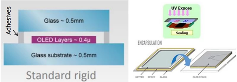
However, the actual OLED material can easily get oxidized by even extremely small quantities of atmospheric moisture and oxygen. Thus, a barrier or seal that protects the sensitive OLED material from oxygen and water is very important. As shown in Figure 1 below, a cover glass is traditionally used as encapsulation for conventional rigid glass substrate OLED. The cover glass has to be permanently bonded on the glass substrate to protect the active OLED layers. This is realized by dispensing an epoxy on the edge of the glass and using a UV LED lamp to cure the epoxy and edge-seal the two glass surfaces.
Process
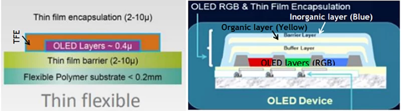
To make a display flexible, the bottom and top glass plates are replaced by flexible substrates, and a flexible Thin Film Encapsulation (TFE) is a must. The thickness of the barrier layer normally lies in the sub-micro range to meet the low permeation requirement of WVTR < 10-6g/m2/day but retains the flexibility. The TFE consists of alternating conformal organic and inorganic layers successively fabricated to achieve low water permeability and high flexibility. While thin inorganic layers work as the barrier layers, organic layers are utilized as “decoupling” layers between inorganic layers to improve the permeation. In addition, organic layers make the structure more robust and flexible since individual inorganic layers in the organic / inorganic multiple layer structure can be kept thinner. The total structure is also more resistant to fragmentation and cracking, when organic layers act as the sealant buffer layer to smooth the substrate.
The TFE fabrication technology includes: 1. Vitex Vacuum Polymer; 2. Inkjet printing (Organic), sputtering (Inorganic); 3. Plasma Enhanced Chemical Vapor Deposition (PECVD)/Atomic Layer Deposition (ALD), etc.
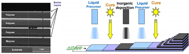
The Vitex process results in flexible encapsulation layers made of alternating Al2O3 and polyacrylate layers as shown in Figure 3 below. While the inorganic Al2O3 layers are sputtered on to the display via plasma, the organic polyacrylate layers are deposited via flash evaporation of the monomer followed by UV curing. The alternating process is repeated to form the multilayer structure.
Although this encapsulation solution shows excellent performance for flexible devices, the elevated complexity presents many challenges for manufacturing process.
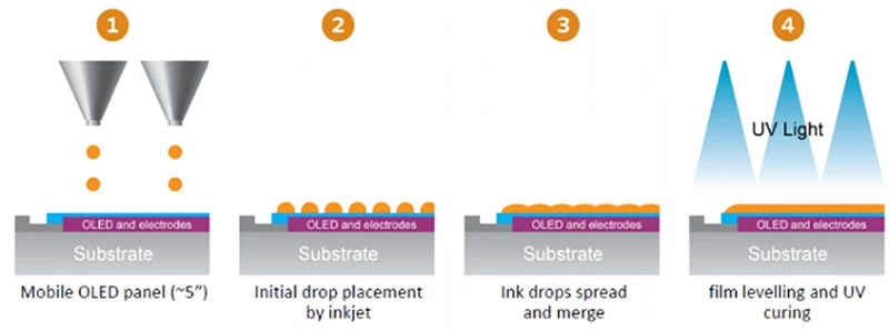
Inkjet-printing based OLED encapsulation started to outsmart Chemical Vapor Deposition (CVD) based OLED encapsulation in terms of process optimization and accuracy, leading to better performances and productivity. It is claimed that inkjet-printed TFE organic interlayers have very high uniformity which eliminate the non-uniform display to the eye (so called “mura”). In addition, since the printing and post print processing are done in a very low H2O and O2 environment, fewer particles are added by the printing process and planarization of the top organic layer is significantly improved to ensure the quality of the second inorganic layer.
As shown in Figure 4 below, after the liquid type organic layer is applied by the inkjet nozzle, a UV curing step is followed to form the crosslink.
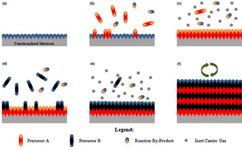
ALD process has been developed to produce very thin, conformal films with control of the thickness. It is a sequential self-terminating CVD process which allows for high-quality coating. It generally consists of sequential alternating pulses of gaseous chemical precursors that react with the substrate. During each gas-surface reaction (half reactions), the precursor is pulsed into a chamber under vacuum for a designated amount of time to allow fully reaction with the substrate surface. Subsequently, the chamber is purged with an inert carrier gas to remove any unreacted precursor or reaction byproducts. The process is cycled until the appropriate film thickness is achieved.
ALD process has many promising features but it suffers from slow deposition rates. No UV LED curing is required in this process.