


 +
+


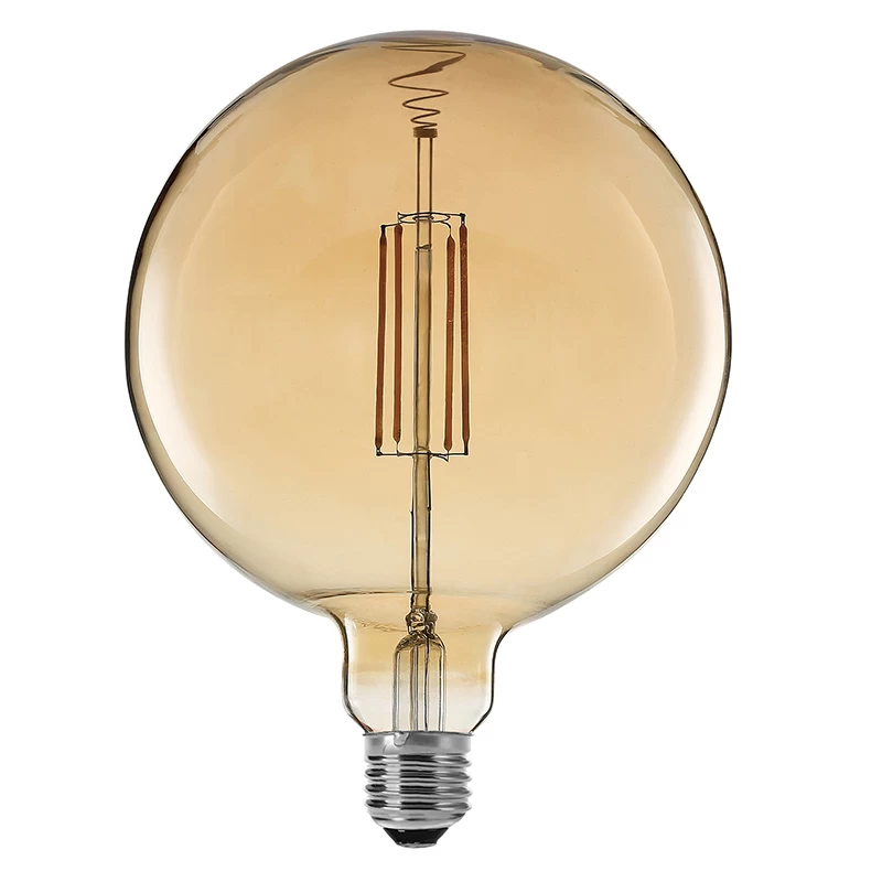
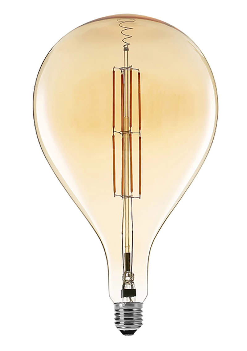
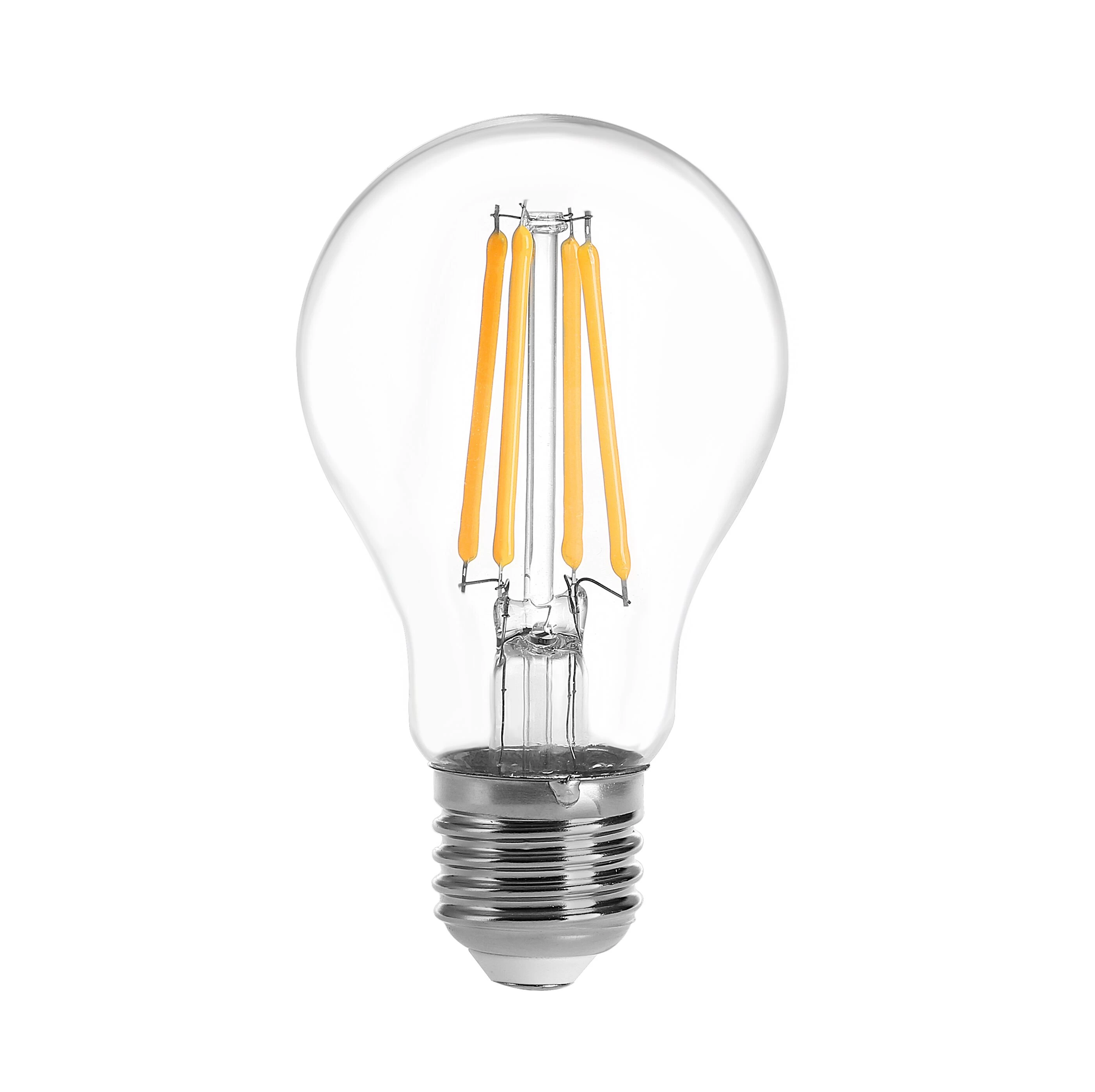
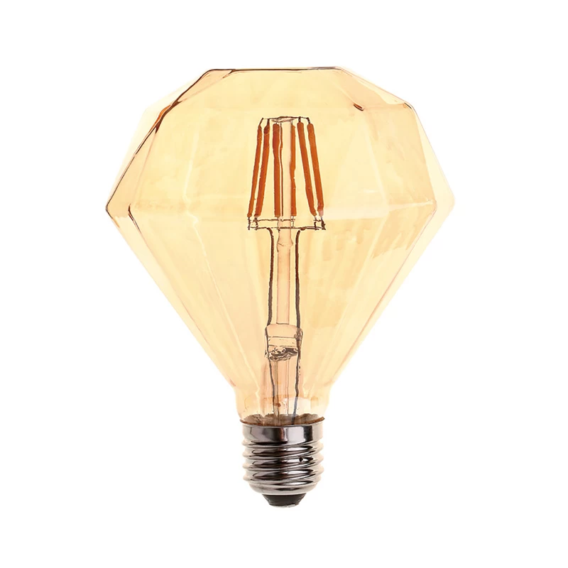


Here are a few things to consider when choosing LED light bulbs...
Efficiency, Colour Temperature, Colour Rendering, Heat Output, lifetime, etc.

Axus Technology and Compound Photonics Partner to Process Monolithic Micro LED Development for AR Ap
Innolite
LEDinside
2020-10-12 15:41:28
Axus Technology, a provider of CMP, wafer thinning and wafer polishing surface-processing solutions for semiconductor applications, announced the collaboration with Compound Photonics (CP, also known as CP Display), a microdisplay solutions developer for AR/MR. The two parties will work to accelerate sub 5 µm pixel Micro LED development to the mass market.
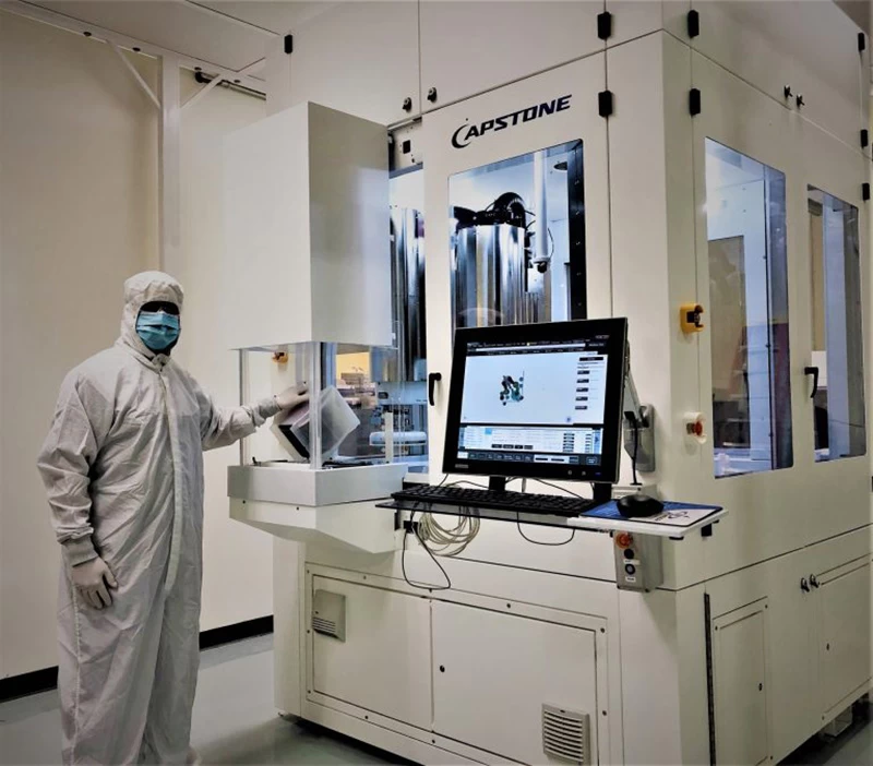
Axus and CP are partnering to integrate critical wafer-scale processes needed for mass-production scale up of CP’s 2 µm pixel, 1080p Micro LED displays for the next generation AR glasses. Specifically, Axus will deploy its Capstone™ CMP system with integrated post-CMP clean to enable wafer planarization and surface preparation process solutions for successful wafer-scale bonding of Micro LED wafers to high-performance CMOS backplanes.
Axus’s CMP processing capability is key to enabling CP’s proprietary, small pixel, epi-substrate agnostic Micro LED integration process scheme. The Capstone CMP system provides the repeatability over multiple wafers and planarity performance within die/wafer to reliably enable bonding of multiple-million micron scale electrical contacts between Micro LED and CMOS backplane wafers. This addresses a critical mass production process requirement for consistently yielding microdisplay modules with required visual uniformity, which is needed for compact, low power, high brightness AR/MR near-eye applications.
Axus and CP have collaborated since early 2020 to develop wafer-scale bonding process integration between Micro LED array and CMOS backplane wafers. The intensified partnership announced lately further demonstrated the commitment from both companies to advance Micro LED display fab processes and integration.
Julie Chao, Product Development Director of CP Display, commented: “We are thrilled to work with Axus to develop CMP and cleaning solutions that enable bonding CP’s CMOS backplane to any sub 5 µm pixel Micro LED wafer. By working together in MiARA, process improvement cycles are naturally accelerated. This is imperative in meeting the market schedule from developers to end customers.”
Micro LED is continuing to emerge as the most potential display solution to meet the critical requirements of AR/MR applications. Innovations in manufacturing process are critical in enabling cost reductions and volume productions for AR/MR headset commercialization.