


 +
+


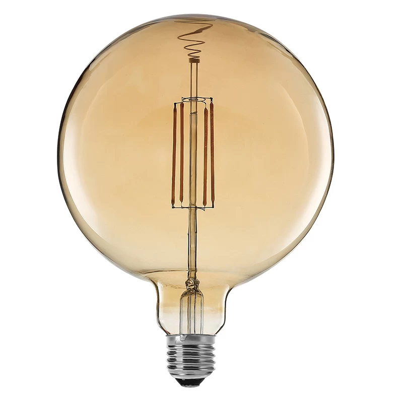


Here are a few things to consider when choosing LED light bulbs...
Efficiency, Colour Temperature, Colour Rendering, Heat Output, lifetime, etc.

What is the technical core of LED lights?
Innotech
Innotech
2018-08-27 10:19:08
LED packaging technology is mostly developed and evolved on the basis of discrete device packaging technology, but it has great speciality. In general, the die of the discrete device is sealed within the package, and the package functions primarily to protect the die and complete the electrical interconnection. The LED package is to complete the output electrical signal, protect the normal operation of the die, output: visible light function, both electrical parameters, optical design and technical requirements, can not simply use the discrete device package for LED.
After entering the 21st century, LED's high efficiency, ultra-high brightness, full colorization continue to develop and innovate. Red and orange LED light effects have reached 100Im/W, green LEDs are 501m/W, and the luminous flux of single LEDs has reached dozens. Im. LED chips and packages no longer follow the traditional design concept and manufacturing mode of Gong. In terms of increasing the light output of the chip, research and development is not limited to changing the amount of impurities in the material, lattice defects and dislocations to improve internal efficiency, and how to improve The internal structure of the die and package enhances the probability of photon emission inside the LED, improves the light efficiency, solves the heat dissipation, optimizes the design of light extraction and heat sink, improves the optical performance, and accelerates the surface mount SMD process. .

1, product packaging structure type
Since the 1990s, LED chip and material fabrication technology has made many breakthroughs in research and development, transparent substrate trapezoidal structure, textured surface structure, chip flip structure, commercial ultra-high brightness (above 1cd) red, orange, Yellow, green, and blue LED products have been asked one after another. As shown in Table 1, in 2000, applications in low- and medium-light flux special lighting were applied. The upper and middle reaches of LED industry have received unprecedented attention, further promoting the downstream packaging technology and industrial development. Different types of package structures and sizes, different luminescent color dies and their two-color or three-color combination can produce a variety of Series, variety, specifications of the product.
The types of LED product package structures are shown in Table 2, and are also classified according to the characteristics of the color of the light, the material of the chip, the brightness of the light, the size, and the like. A single die generally constitutes a point source, and a plurality of die assemblies generally constitute a surface source and a line source for information, status indication, and display. The illuminating display also uses a plurality of dies, through appropriate connections of the dies (including series and Parallel) combined with a suitable optical structure to form the illumination segment and the illumination point of the illuminated display. Surface mount LEDs can gradually replace pin-type LEDs, and the application design is more flexible. It has occupied a certain share in the LED display market and has an accelerated development trend. Some solid-state lighting sources have been launched, which will become the medium and long-term development direction of LEDs in the future.
2, lead package
The LED foot package uses lead frames as pins for various package types. It is the first package structure successfully developed on the market. The variety of products is high, the technology maturity is high, and the structure and reflective layer inside the package are still being improved. Standard LEDs are considered by most customers to be the most convenient and economical solution in the display industry. Typical LEDs are housed in an enclosure that can withstand 0.1W of input power, 90% of which is pinned by the negative pole. The rack is distributed to the PCB and then released into the air. How to reduce the temperature rise of the pn junction during operation is a must for packaging and application. The encapsulating material is mostly made of high-temperature curing epoxy resin, which has excellent optical performance, good process adaptability, high product availability, and can be made into a transparent or colorless transparent and colored scattering or colorless lens package, different lenses. The shape constitutes various shapes and sizes. For example, the circular shape is divided into several types according to the diameter: Φ2mm, Φ3mm, Φ4.4mm, Φ5mm, Φ7mm, etc., and different components of the epoxy resin can produce different illuminating effects. The color point light source has a variety of different package structures: the ceramic base epoxy resin package has better working temperature performance, the lead can be bent into a desired shape, and the volume is small; the metal base plastic reflective cover type package is an energy-saving indicator light. Suitable for power indication; flashing CMOS oscillating circuit chip and LED die package, can produce self-generated flashing light with strong visual impact; two-color type consists of two different luminescent color dies, packaged in the same epoxy In the resin lens, a third mixed color can be obtained in addition to the two colors, which is widely used in a large-screen display system, and can be packaged to form a two-color display device; the voltage type is a combination of a constant current source chip and an LED die. Can directly replace the various voltage indicators of 5-24V. The surface light source is formed by bonding a plurality of LED dies to a predetermined position of the micro PCB board, and is formed by using a plastic reflective frame cover and potting the epoxy resin. The different designs of the PCB board determine the arrangement and connection manner of the outer leads, and the double row is straight. Insert and single-row inline and other structural forms. Point and surface light sources have been developed in hundreds of package shapes and sizes for the market and customers.
The LED light-emitting display can be composed of a digital tube or a meter tube, a symbol tube, and a rectangular tube to form various products, and is designed into various shapes and structures according to actual needs. Take the digital tube as an example, there are three kinds of package structures, such as a reflector cover, a single-chip integrated type, and a single seven-segment type. The connection mode includes a common anode and a common cathode. One is a commonly known digital tube, and two or more. Generally referred to as a display. The reflector type has the characteristics of large font, material saving, and flexible assembly. It is generally made of white plastic into a seven-section housing with a reflective cavity, and a single LED die is bonded to the seven reflective chambers of the reflector. On the PCB board that is aligned with each other, the center position of the bottom of each reflection cavity is the light-emitting area formed by the die, and the lead wire is bonded by a pressure welding method, and the epoxy resin is dropped in the reflection cover, and the PCB board of the die is bonded. Bonded in place and then cured. Reflective cover type is divided into air seal and solid seal. The former uses epoxy resin with scattering agent and dye, and is mostly used for unit and double-position devices; the latter is covered with color filter and uniform film, and is in the die and The bottom plate is coated with transparent insulating glue to improve the light-emitting efficiency, and is generally used for digital display of four or more digits. The monolithic integrated method is to fabricate a large number of seven-segment digital display graphic dies on a luminescent material wafer, and then dicing into a single-patterned dicing die, bonding, pressure-welding, and encapsulating a lens with a lens (commonly known as a fisheye lens). A single seven-segment type of large-area LED chip that has been fabricated into a light-emitting strip containing one or more dies, so that the same seven pieces are bonded to the digital-shaped slash frame, and are pressure-welded and epoxy. Resin package construction. The monolithic and single strip features are miniaturized and can be used in dual in-line packages, mostly for specialty products. The LED light column display houses 101 dies (up to 201 dies) on a 106mm length circuit board. It is a high-density package that uses optical refraction principles to image the point source through 13-15 strips of transparent cover. The dot-to-line display of each die is completed, and the packaging technology is more complicated.
The electroluminescence mechanism of the semiconductor pn junction determines that it is impossible for LED to produce white light with continuous spectrum. At the same time, it is impossible for a single LED to produce more than two kinds of high-brightness monochromatic light. It can only be used for packaging with fluorescent substances, blue or ultraviolet LEDs. The phosphor is coated on the die to indirectly generate a broadband spectrum, and the white light is synthesized; or a plurality of (two or three or more) dice of different color lights are packaged in one component casing, and the white LED is formed by mixing the color lights. . Both methods have been put into practical use. In 2000, Japan produced 100 million white LEDs, which developed into a class of products that stably emit white light. The design of multiple white LEDs was not required to meet the luminous flux requirements. Lord, the pursuit of a new electric light source.
3, surface mount package
In 2002, surface mount packaged LEDs (SMD LEDs) were gradually accepted by the market and gained a certain market share. From lead package to SMD, it conformed to the development trend of the whole electronics industry, and many manufacturers introduced such products.
Most of the early SMD LEDs were modified with SOT-23 with a transparent plastic body. The outer dimensions were 3.04×1.11mm, and the reel-type container was taped. Based on SOT-23, the SLM-125 series with high-brightness SMD with lens and SLM-245 series LED are developed. The former is monochromatic illumination, and the latter is two-color or three-color illumination. In recent years, SMD LED has become a development hotspot, which solves the problems of brightness, viewing angle, flatness, reliability, consistency, etc., using lighter PCB board and reflective layer material, which needs to be filled in the reflective layer. Fewer epoxy resin and remove the heavier carbon steel material pins. By reducing the size and weight, you can easily reduce the weight of the product by half, and finally make the application perfect. Especially suitable for indoor, semi-outdoor full color display. Screen application.
Table 3 shows several dimensions of common SMD LEDs, as well as the best viewing distance calculated from the dimensions (plus the necessary clearance). The pad is an important channel for heat dissipation. The SMD LED data provided by the manufacturer is based on a 4.0×4.0mm pad. The reflow soldering can be used to design the pad to be equal to the pin. Ultra-high-brightness LED products can be packaged in PLCC (plastic package with lead chip carrier)-2, the external dimensions are 3.0×2.8mm, and the high-brightness die is assembled by a unique method. The thermal resistance of the product is 400K/W, which can be pressed. CECC soldering, its luminous intensity is 1250mcd at 50mA driving current. The seven-segment one, two, three and four digital SMD LED display devices have a character height of 5.08-12.7mm and a wide display size range. The PLCC package avoids the manual insertion and pin alignment processes required for the seven-segment digital display of the pin, and meets the production requirements of the automatic pick-and-place device. The application design space is flexible and the display is bright and clear. The multi-color PLCC package features an external reflector that can be easily combined with an LED or light guide to replace the current transmissive optical design with a reflective version to provide uniform illumination over a wide area, developed at 3.5V, 1A drive Power SMD LED package operating under conditions.
4, power package
The LED chip and package are developed in the direction of high power. Under the high current, the luminous flux is 10-20 times larger than that of the Φ5mm LED. The effective heat dissipation and non-degraded packaging materials must be used to solve the light decay problem. Therefore, the package and the package are also the key. Technology, LED packages that can withstand several W power have emerged. 5W series white, green, blue green, blue power LEDs have been available since the beginning of 2003. The white LED light output reaches 1871m, the light efficiency is 44.31m/W green light decay problem, and the LED that can withstand 10W power is developed. The area tube; the size of the crucible is 2.5×2.5mm, it can work under the current of 5A, and the light output reaches 2001m. It has great development space as a solid illumination source.
The Luxeon series power LEDs are flip-chip soldered to the silicon carrier with solder bumps, and then the flip-chip soldered silicon carrier is placed in the heat sink and the package, and the bonding leads are packaged. This package is optimized for light extraction efficiency, heat dissipation performance, and increased operating current density. Its main features: low thermal resistance, generally only 14 ° C / W, only 1 / 10 of conventional LED; high * high flexibility, the package is filled with a stable flexible gel, in the range of -40-120 ° C, will not be The internal stress generated by sudden temperature changes disconnects the gold wire from the lead frame and prevents the epoxy lens from turning yellow. The lead frame is not stained by oxidation. The optimal design of the reflector cup and lens makes the radiation pattern controllable. The optical efficiency is the highest. In addition, its output optical power, external quantum efficiency and other properties are excellent, and the LED solid light source has been developed to a new level.
The package structure of the Norlux series of power LEDs is a multi-chip combination of a hexagonal aluminum plate as a base (which makes it non-conductive). The base has a diameter of 31.75 mm, and the light-emitting area is located at the center thereof, and the diameter is about 0.375 × 25.4 mm. 40 LED dies, the aluminum plate is also used as a thermal lining. The bonding wires of the die are connected to the positive and negative electrodes through two contact points made on the base, and the number of aligned dies on the base is determined according to the required output optical power, and the packaged ultra-high brightness AlGaInN and AlGaInP can be combined. The die, which emits light in a single color, color or synthetic white, is finally encapsulated in an optically designed shape with a high refractive index material. The package adopts a conventional high-density package with high density, high light extraction efficiency, low thermal resistance, better protection of the die and bonding wires, and high light output power under high current, which is also a promising future. LED solid light source.
In the application, the packaged product can be assembled on a metal core PCB with aluminum interlayer to form a power density LED. The PCB is used as the wiring for the device electrode connection, and the aluminum core interlayer can be used as a thermal lining. Higher luminous flux and photoelectric conversion efficiency. In addition, the packaged SMD LEDs are small in size and can be flexibly combined to form a variety of illumination sources such as module type, light guide type, concentrating type, and reflective type.
The thermal characteristics of power LEDs directly affect the operating temperature, luminous efficiency, wavelength of illumination, and lifetime of LEDs. Therefore, the packaging design and manufacturing technology of power LED chips are particularly important.